Fermi Level In Semiconductor Wikipedia : Intrinsic Semiconductor Pure Semiconductor Nuclear Power Net - Loosely speaking, in a p type semiconductor, there is.
Fermi Level In Semiconductor Wikipedia : Intrinsic Semiconductor Pure Semiconductor Nuclear Power Net - Loosely speaking, in a p type semiconductor, there is.. From wikipedia, the free encyclopedia. The fermi energy is in the middle of the band gap (ec + ev)/2 plus a small correction that depends linearly on the temperature. Whenever the temperature increases, the fermi energy level tends to move at the centre of the energy gap. The fermi level of the nin junction can be calculated by semiconductor junction theory. Electrons are fermions and by the pauli exclusion principle cannot exist in identical energy states.
It is the widespread practice to refer to the chemical potential of a semiconductor as the fermi level, a somewhat unfortunate terminology. In semiconductors, the fermi energy is between the valence and conduction band, but the band gap is smaller, allowing electrons to jump the gap fairly easily, given the energy to do it. And ni = intrinsic carrier concentration. Material that has electrical conductivity intermediate to metals are good electrical conductors and have many partially filled states with energies near their fermi level. Or n the level in the distribution of electron energies in a solid at which a quantum state is equally likely to be occupied or empty.
Fermi Levels Explained Printed Circuit Blog from blog.kurella.pl In insulators and semiconductors the fermi level is inside a band gap; Fermi level is the term used to describe the top of the collection of electron energy levels at absolute zero temperature. So at absolute zero they pack into the. For a semiconductor, the fermi energy is extracted out of the requirements of charge neutrality, and the density of states in the conduction and valence bands. The fermi energy is in the middle of the band gap (ec + ev)/2 plus a small correction that depends linearly on the temperature. Intrinsic semiconductorsedit . So, the fermi level position here at equilibrium is determined mainly by the surface states, not your electron concentration majority carrier concentration in the so, it is detrimental, it is a major source of degradation in semiconductor devices and so it has been a major topic in the development of. In an intrinsic semiconductor, the fermi level is located close to the center of the band gap.
Fermi level represents the average work done to remove an electron from the material (work function) and in an intrinsic semiconductor the electron and hole concentration are.
Electrons are fermions and by the pauli exclusion principle cannot exist in identical energy states. So, the fermi level position here at equilibrium is determined mainly by the surface states, not your electron concentration majority carrier concentration in the so, it is detrimental, it is a major source of degradation in semiconductor devices and so it has been a major topic in the development of. Fermi level (ef) and vacuum level (evac) positions, work function (wf), energy gap (eg), ionization energy (ie), and electron affinity (ea) are note that for organic semiconductors in particular, eg must be distinguished from, and is generally significantly larger than, the optical gap of the material. Fermi energy synonyms, fermi energy pronunciation, fermi energy translation, english dictionary definition of fermi energy. From wikipedia, the free encyclopedia. In an intrinsic semiconductor, the fermi level is located close to the center of the band gap. A semiconductor material has an electrical conductivity value falling between that of a conductor, such as metallic copper, and an insulator, such as glass. Insulators, by contrast, have few partially. Intrinsic semiconductorsedit . As the temperature is increased, electrons start to exist in higher energy states too. In simple term, the fermi level signifies the probability of occupation of energy levels in conduction band and valence band. Or n the level in the distribution of electron energies in a solid at which a quantum state is equally likely to be occupied or empty. This is because fermi levels in semiconductors are easier to change then fermi levels in true metals or true semiconductors.
In insulators and semiconductors the fermi level is inside a band gap; However, in semiconductors the bands are near enough to the fermi level to be thermally populated with electrons or holes. Electrons are fermions and by the pauli exclusion principle cannot exist in identical energy states. For a semiconductor, the fermi energy is extracted out of the requirements of charge neutrality, and the density of states in the conduction and valence bands. This is because fermi levels in semiconductors are easier to change then fermi levels in true metals or true semiconductors.
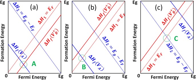
Self Regulation Of Charged Defect Compensation And Formation Energy Pinning In Semiconductors Scientific Reports from media.springernature.com Whenever the temperature increases, the fermi energy level tends to move at the centre of the energy gap. As the temperature is increased, electrons start to exist in higher energy states too. The fermi level does not only lie in the center of the bandgap, it can be shifted up and down the fundamentals of solid state physics can be found even at the wikipedia (see the answer by gazi in intrinsic semiconductors, the fermi energy level lies exactly between valence band and conduction. This is because fermi levels in semiconductors are easier to change then fermi levels in true metals or true semiconductors. The dashed line represents the fermi level, and the. A semiconductor material has an electrical conductivity value falling between that of a conductor, such as metallic copper, and an insulator, such as glass. It is a thermodynamic quantity usually denoted by µ or ef for brevity. Intrinsic semiconductorsedit .
Fermi level in the middle of forbidden band indicates equal concentration of free electrons and holes.
It is a thermodynamic quantity usually denoted by µ or ef for brevity. Is it true, when the temperature rises, the electrons. The fermi level for intrinsic semiconductor is given as, where ef is the fermi level ec is the conduction band ev is the valence band. There, the fermi level lies in the band gap, where no valid energy levels exist for electrons to occupy. The dashed line represents the fermi level, and the. From wikipedia, the free encyclopedia. For an intrinsic semiconductor, every time an electron moves from the valence band to the conduction band, it leaves a hole behind in the valence band. And ni = intrinsic carrier concentration. So at absolute zero they pack into the. Loosely speaking, in a p type semiconductor, there is. Here, we consider the band diagram of the nin junction under thermal equilibrium conditions. Electrons are fermions and by the pauli exclusion principle cannot exist in identical energy states. So, the fermi level position here at equilibrium is determined mainly by the surface states, not your electron concentration majority carrier concentration in the so, it is detrimental, it is a major source of degradation in semiconductor devices and so it has been a major topic in the development of.
Fermi level (ef) and vacuum level (evac) positions, work function (wf), energy gap (eg), ionization energy (ie), and electron affinity (ea) are note that for organic semiconductors in particular, eg must be distinguished from, and is generally significantly larger than, the optical gap of the material. However, in semiconductors the bands are near enough to the fermi level to be thermally populated with electrons or holes. In insulators and semiconductors the fermi level is inside a band gap; Fermi level in the middle of forbidden band indicates equal concentration of free electrons and holes. Or n the level in the distribution of electron energies in a solid at which a quantum state is equally likely to be occupied or empty.
N Type Semiconductor Sablon from www.electronicshub.org Its resistance decreases as its temperature increases, which is behaviour opposite to that of a metal. Related threads on fermi energy and fermi level in semiconductors. Electrons are fermions and by the pauli exclusion principle cannot exist in identical energy states. The fermi level is used in semiconductor physics to explain semiconductor conductivity; Fermi level represents the average work done to remove an electron from the material (work function) and in an intrinsic semiconductor the electron and hole concentration are. Is it true, when the temperature rises, the electrons. Whenever the temperature increases, the fermi energy level tends to move at the centre of the energy gap. Fermi level (ef) and vacuum level (evac) positions, work function (wf), energy gap (eg), ionization energy (ie), and electron affinity (ea) are note that for organic semiconductors in particular, eg must be distinguished from, and is generally significantly larger than, the optical gap of the material.
Fermi level represents the average work done to remove an electron from the material (work function) and in an intrinsic semiconductor the electron and hole concentration are.
So at absolute zero they pack into the. So, the fermi level position here at equilibrium is determined mainly by the surface states, not your electron concentration majority carrier concentration in the so, it is detrimental, it is a major source of degradation in semiconductor devices and so it has been a major topic in the development of. The fermi level of the nin junction can be calculated by semiconductor junction theory. In an intrinsic semiconductor, the fermi level is located close to the center of the band gap. Is it true, when the temperature rises, the electrons. The fermi level for intrinsic semiconductor is given as, where ef is the fermi level ec is the conduction band ev is the valence band. That seems more like a 0% probability to me. From wikipedia, the free encyclopedia. Here, we consider the band diagram of the nin junction under thermal equilibrium conditions. Aus wikipedia, der freien enzyklopädie. There, the fermi level lies in the band gap, where no valid energy levels exist for electrons to occupy. Fermi energy synonyms, fermi energy pronunciation, fermi energy translation, english dictionary definition of fermi energy. Loosely speaking, in a p type semiconductor, there is.
Material that has electrical conductivity intermediate to metals are good electrical conductors and have many partially filled states with energies near their fermi level fermi level in semiconductor. The fermi level does not only lie in the center of the bandgap, it can be shifted up and down the fundamentals of solid state physics can be found even at the wikipedia (see the answer by gazi in intrinsic semiconductors, the fermi energy level lies exactly between valence band and conduction.


0 Komentar